1.1 Fundamentals of a Computer
A computer has three key components:
- Computation
- Communication
- Storage/Memory
Transformation Hierarchy
The transformation hierarchy covers all 9 layers of computing.
![]()
The problem-solving process involves several layers of abstraction and transformation:
- Problem: The initial task to be solved.
- Algorithm: A finite, definite, and effectively computable procedure.
- Finiteness: Algorithm terminates after a finite number of steps.
- Definiteness: Each step is precisely defined and unambiguous.
- Effective Computability: Each step can be carried out by a computer.
- Program/Language: Implementation of the algorithm in a specific programming language.
- System Software: Includes Virtual Machines (VMs), Operating Systems (OS), Memory Managers, etc., providing a platform for program execution.
- Instruction Set Architecture (ISA): The interface between software and hardware. It defines the instructions the hardware understands. The programmer relies on the hardware to correctly implement the ISA.
- Microarchitecture: The specific implementation of the ISA (e.g., x86, ARM, RISC-V). Different microarchitectures can implement the same ISA with varying performance and power characteristics.
- Logic: Digital logic circuits that implement the microarchitecture.
- Devices: Physical devices, such as transistors, that realize the logic gates.
- Electrons: The fundamental particles manipulated to perform computation.
Trade-offs
There are tradeoffs between power, performance, size, etc… to be made that will govern the type of architecture chosen.
We can specialise our system in order to make it faster at certain tasks, losing the general-purpose computing speed: see the difference between ASICS and consumer desktop hardware CPUs.
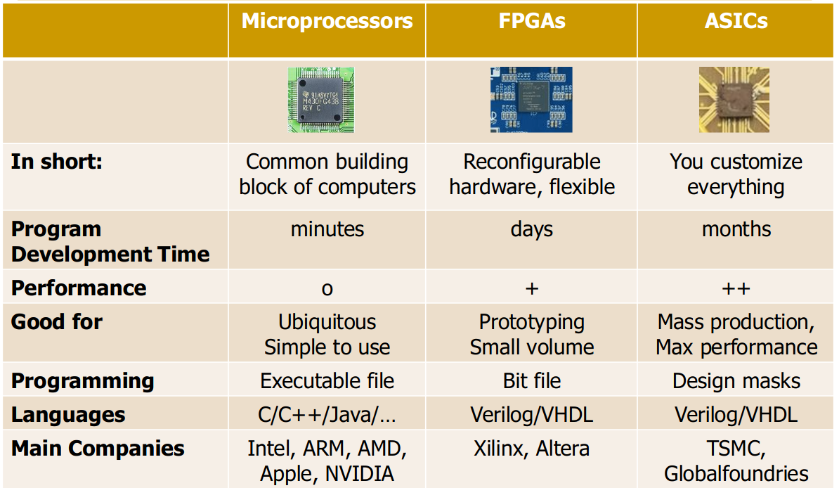
We will learn how Microprocessors work in this course, by programming FPGAs to emulate them in Verilog.
1.2 Transistors
MOS Transistor
MOS is “Metal Oxide Semiconductor”. We combine the metal conductor with an oxide insulator to get a transistor.
MOS transistor’s electrical properties are below our lowest level of abstraction.
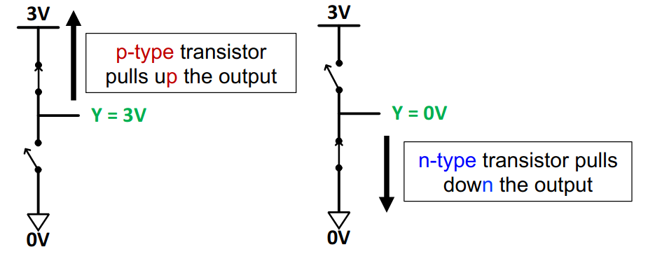
N-Type & P-Type
There are two types of MOS transistors: n-type and p-type.
They operate “logically” like a switch.
N-Type: Circuit is closed when the gate is supplied with 3V (pull down)
P-Type: Circuit is closed when the gate is supplied with 0V (pull up)
![]()
An nMOS acts as a normally-OFF switch:
- Gate HIGH (relative to Source, exceeding Threshold Voltage VT): A positive gate voltage attracts electrons, forming a conductive n-channel between source and drain. The switch is ON.
- Gate LOW: No channel forms. The switch is OFF.
Characteristics of an nMOS: - Strong ‘0’ Passer: Efficiently pulls an output node to GND.
- Weak ‘1’ Passer: When passing Vdd, the output only reaches Vdd−VT due to the threshold voltage drop, resulting in a degraded high signal.
A pMOS also acts as a normally-OFF switch, but with inverted gate logic:
- Gate LOW (relative to Source, significantly below by its threshold ∣VTp∣): A negative gate voltage attracts holes, forming a conductive p-channel. The switch is ON.
- Gate HIGH: No channel forms. The switch is OFF.
Characteristics of a pMOS: - Strong ‘1’ Passer: Efficiently pulls an output node to Vdd.
- Weak ‘0’ Passer: When passing GND, the output only reaches GND+∣VTp∣ (i.e., cannot fully reach GND), resulting in a degraded low signal.
1.3 Logic Gates
We can use these transistors to implement Logic Gates.
Modern computers mix both n-type and p-type transistors which is the basis of CMOS (Complimentary MOS) technology (nMOS + pMOS = CMOS).
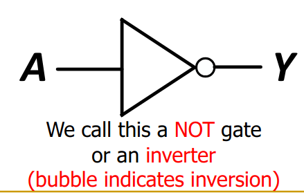
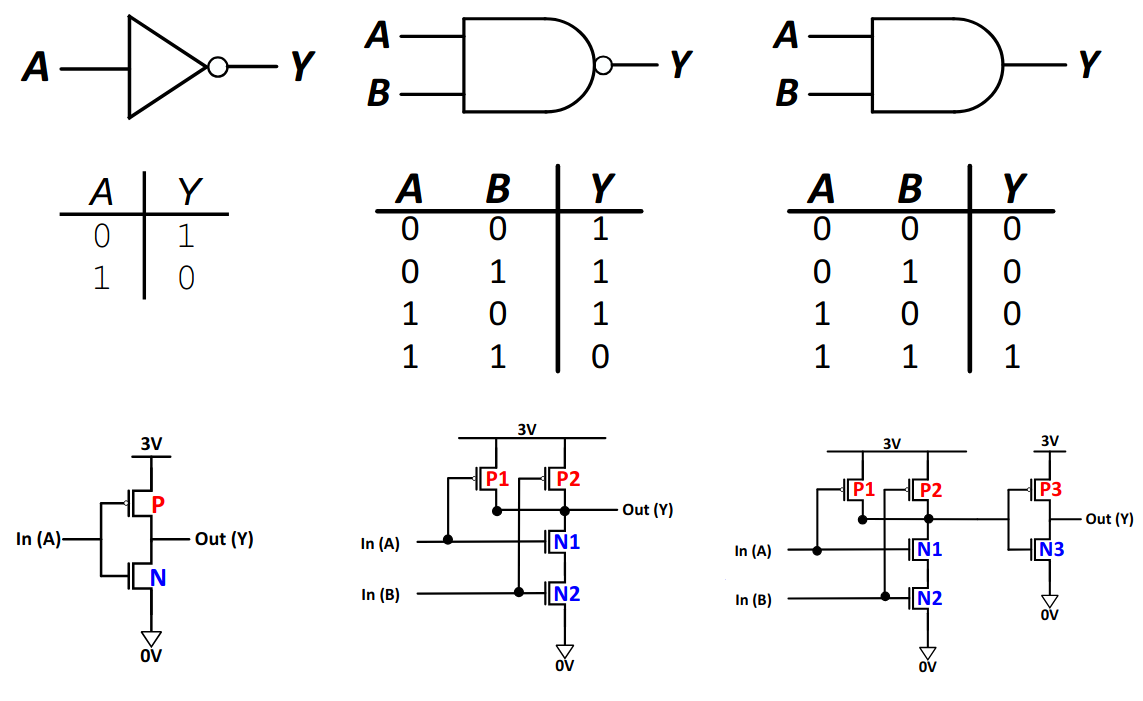
NOT Gate
The note gate uses 1 p-type transistor and 1 n-type transistor, wired to the same input.
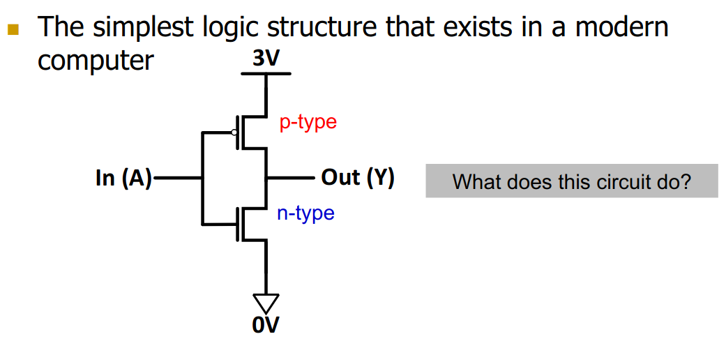
When the input is low, the p-type pulls up the voltage from the 3V source, inverting the signal. When the input is high, the n-type transistor connects the output to ground, pulling down the voltage.
We interpret the voltages as logical values, in order to use this as a logical not gate.
The bubble after the triangle indicates inversion (This bubble can be seen on other gates to indicate inversion as well).
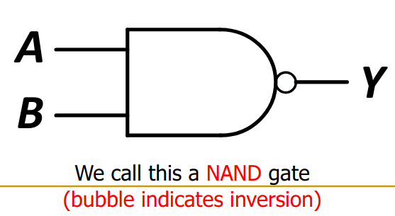
NAND Gate
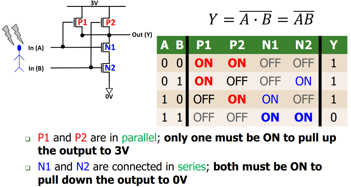
The NAND gate is modelled using 4 transistors. Two parallel p-type transistors and two n-type in series.
We can then make an AND gate using one NAND and a NOT in series.
Overview
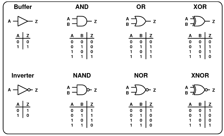
We now learned about these 3 gate types. NAND is logically complete, meaning we can build all necessary logical operations from NAND gates (using the fact that all expressions have a DNF / CNF form).
And some more general gates and their truth tables:
1.4 CMOS
The general form of any logic gate such as NOT, NAND, NOR, etc… is that of a CMOS gate structure.
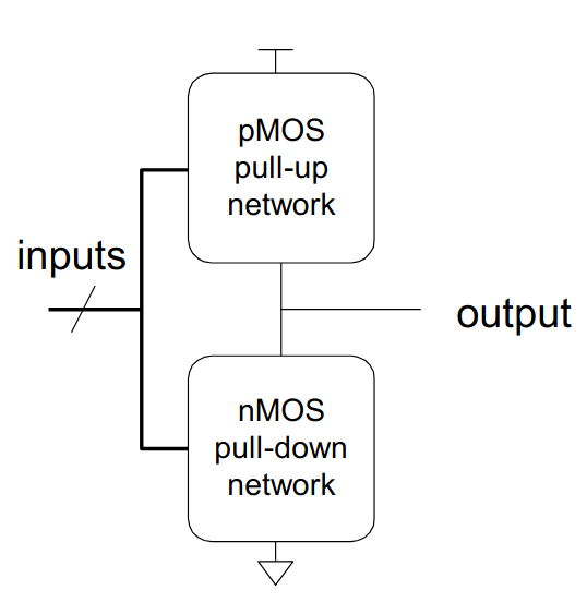
It is made up of two networks, a pMOS pull-up network and a nMOS pull-down network.
These networks can be complex transistor arrangements (either parallel or in series):
- parallel means that the network is ON if one of the transistors is ON
- series means that the network is ON if all of the transistors are ON
Exactly one network should be ON and the other should be OFF at any given time!
- if both are ON at the same time ⇒ Short-Circuit!
- A short-circuit may damage the equipment as current flows freely and without resistance from power supply to ground.
- Output voltage of the gate is undefined → Issues with downstream logic
- if both are OFF at the same time ⇒ output is floating (sometimes useful) which means that it’s undefined
- Also called high-impedance state.
Why this CMOS Structure?
Due to transistor imperfections, they don’t behave like perfect switches.
- as stated before, pMOS exhibit a voltage drop when trying to pull a node to ground, i.e. they don’t conduct 0s well.
- nMOS are poor at passing 1s (high voltage) and exhibit a voltage drop when pulling up.
By using pMOS in the Pull-Up-Network (PUN) and nMOS in the PDN, we overcome these limitations.
Due to electrons higher mobility, nMOS transistors are generally faster than pMOS. Filling holes due to electron “hopping” takes longer than electrons simply moving around (passing negative charge).
Latency
Transistors in series are slower than transistors in parallel. The series construction increases resistance and hinders flow - less resistance = quicker signal transition.
1.5 Power Consumption
We can estimate the power consumption of a circuit using two concepts: dynamic power consumption and static power consumption.
Dynamic Power Consumption
This is power used to charge capacitance (our circuit is essentially one big capacitor) as signals change: are the involved terms.
- is the capacitance of the circuit (wires and gates)
- is the supply voltage
- is the charging frequency of the capacitor (basically clock speed)
Each time we have a signal transition, the capacitance needs to be charged to .
Static Power Consumption
The static power is consumed due to leakage current inherent to the architecture.
It is estimated using which is the supply voltage times the leakage current.
The total energy consumption is then .