Memory is a very important component, arguably more so than the actual compute.
- Area: On the chip, modern CPUs often have more cache area than the computation parts.
- Efficiency: 100-1000x more energy for memory interconnect, etc… than actual computation
- Idle most CPUs spend most of the time idle, waiting on memory
- Vulnerability
- Rowhammer
- becomes a bigger issue with more constrained physical space → more memory
- Failures
- more memory = more trouble (Facebook study by Mutlu)
- Rowhammer
We put a lot of effort into working around memory latency/bandwidth → OoO, memory banking, …
22.0 Memory Hierarchy
We use different types of memory for different use-cases in the computer.
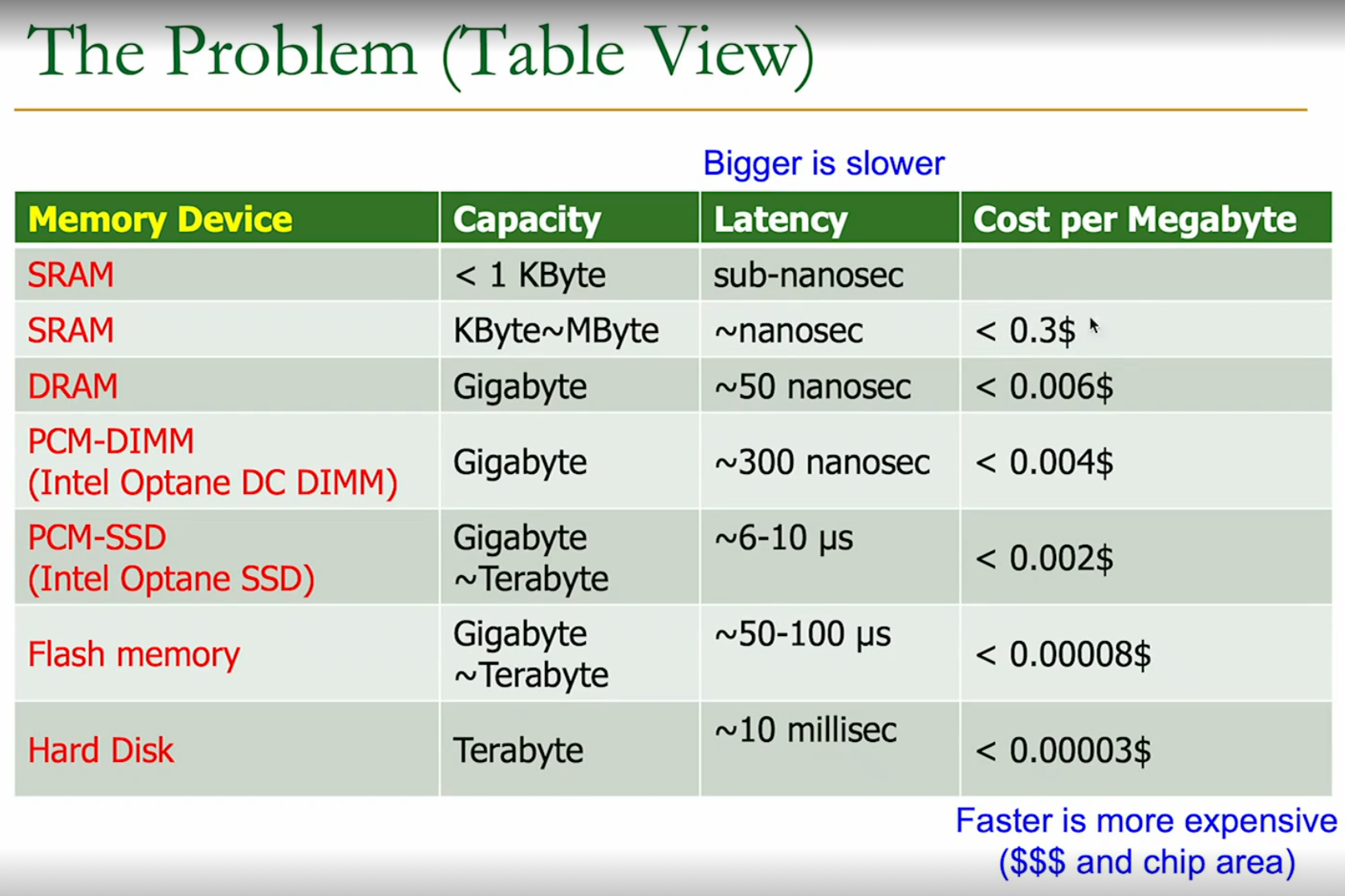
We deploy them at multiple “levels” (hierarchies) → keep the relevant data in the faster memory closer to the processor.
22.1 Physical Memory
22.1.1 Different Technologies
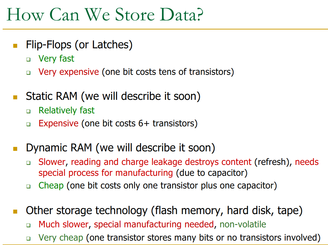
DRAM:
- slower access → capacitor
- higher density
- requires refresh
- specialised manufacturing (for capacitor)
- as you scale down the capacitor → sensing becomes harder
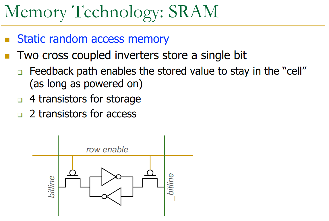
SRAM: - faster access (no capacitor)
- higher cost
- no refresh
- → SRAM is used inside the CPU because it’s the same manufacturing process
- used in caches
We will focus on DRAM here.
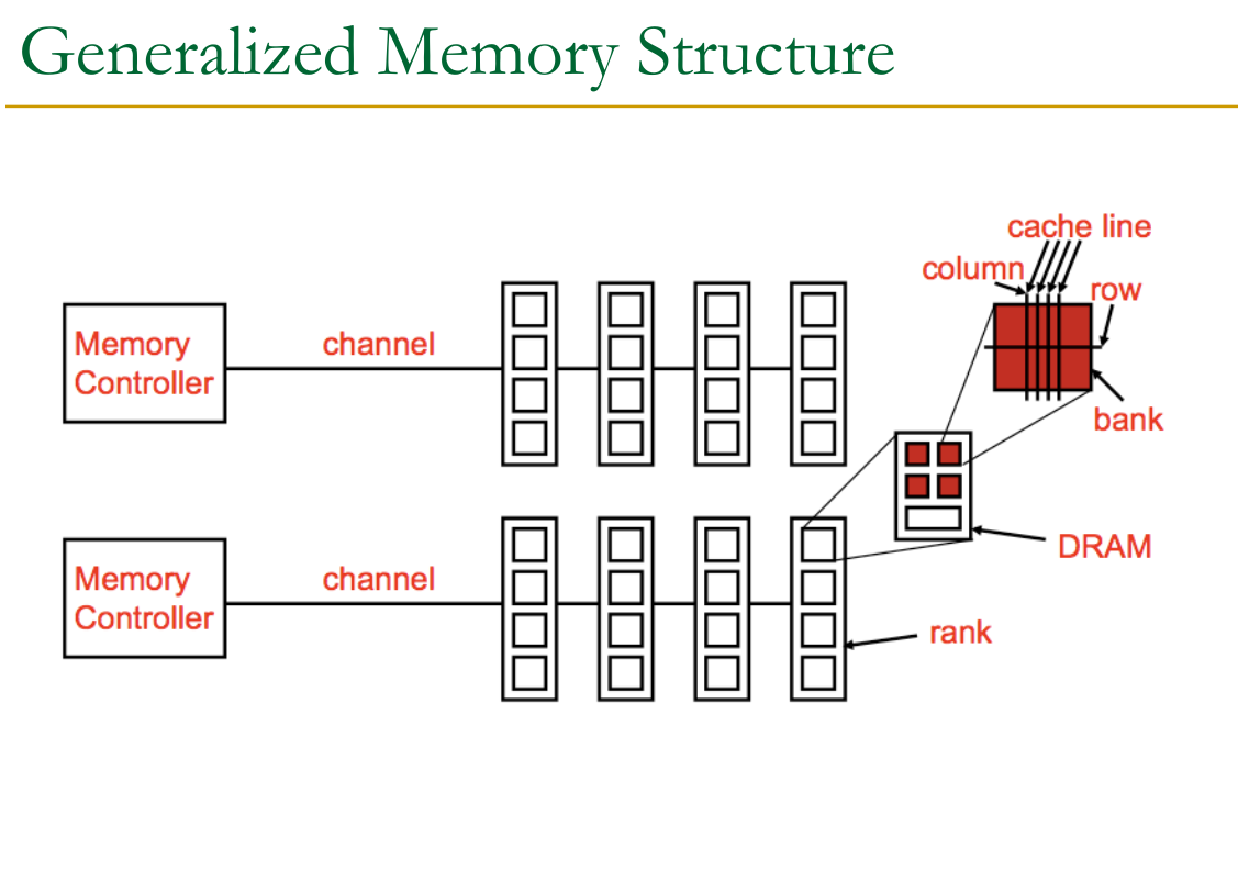
Memory Organisation Memory is organised into sub-structures to improve performance.
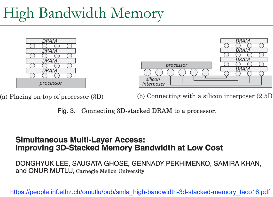
HBM allows for even higher bandwidth by stacking more memory → decreases time.
22.1.1 Recap
A few things to keep in mind:
- DRAM Page != virtual memory page
- Cache block → memory transferred when accessing an address
- cache line → where it is stored on the CPU cache, with the valid bit / dirty bit, etc…
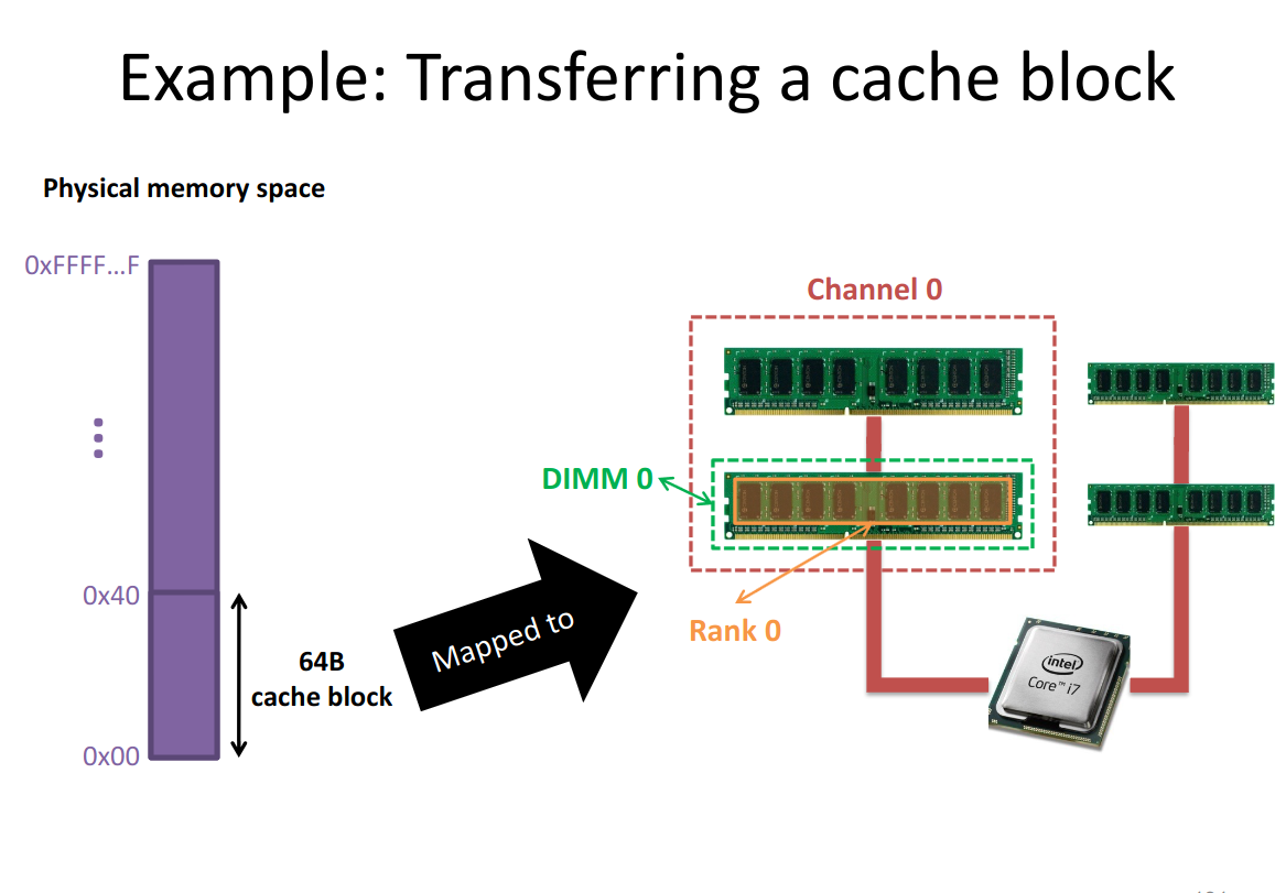
22.2 DDRX RAM
Separated into: Channel → Rank → Bank → Subarray → Mat
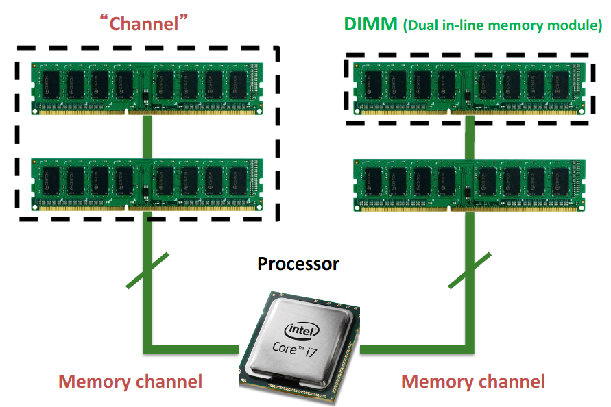
Each channel is truly independent. But inside a channel, all DIMMs share the same 0:63 bit line (there are 64 pins for data on a DIMM → but there are more for other things…).
22.3 Ranks
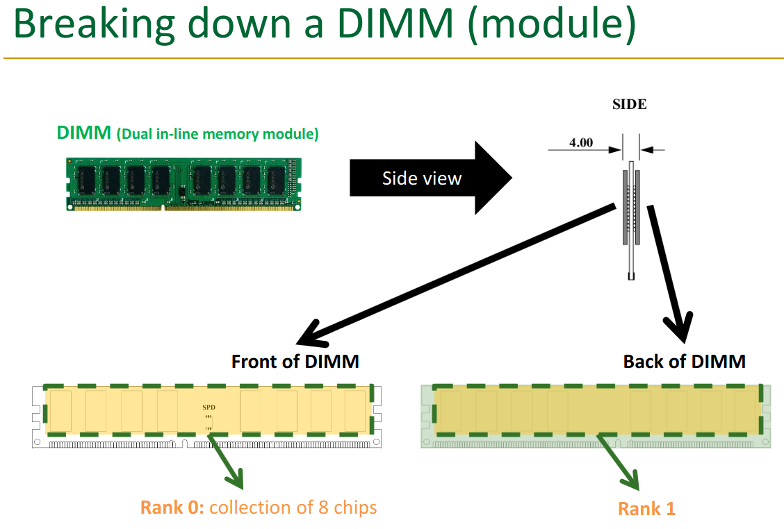
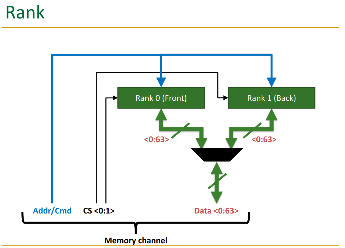
Each side of a DIMM is one rank.
The ranks get the same command though, they aren’t “data parallel”.
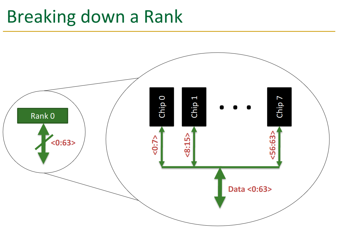
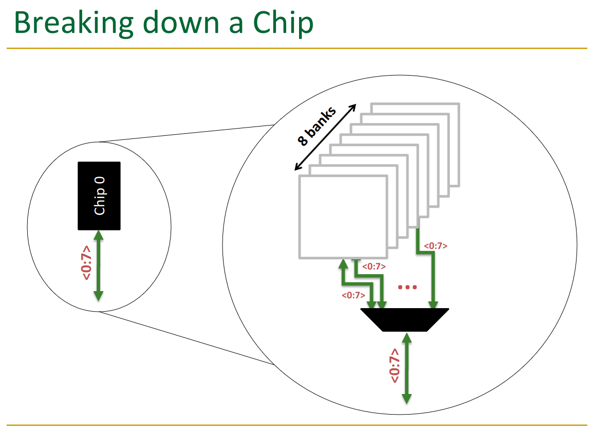
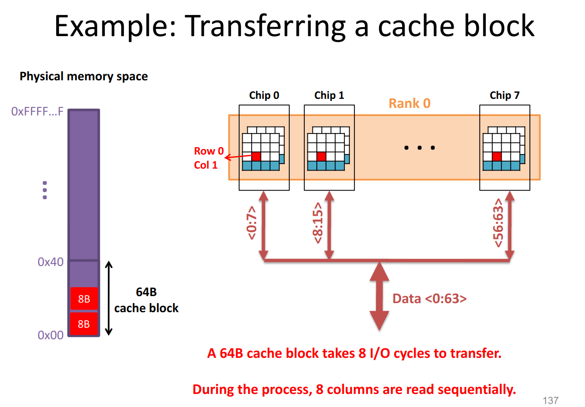
Notice one rank has 8 chips → this means each chip is delivering 8 bits, which get merged together. The data is thus “sharded” across the chips.
Rank each rank has the 8 chips on it, each delivering 8 bits:
22.4 Banks
Banking reduces the latency of memory access (through latency overlap) and enables “parallel access”. We can read from 1 bank per cycle, but by rotating through them, we decrease wait time.
→ critical to get right interleaving accross the banks.
You can only get data from one bank at a time → multiplexer controls this.
But, you can switch between them on each cycle.
22.5 Array
We measure the width height of a memory array:
- width = “word size”
- height/depth = capacity
So a 4x3 memory array has 4 locations (words), each storing 3 bits.
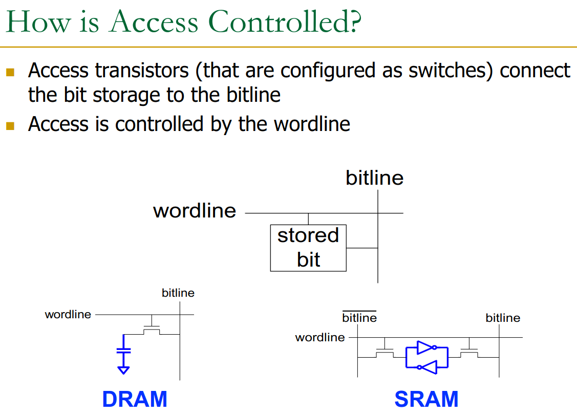
When a wordline is activated, the access transistors connect the bit storage to the bitline.
Since the width of the usual array is many times larger than the 64 bits (1-2kb wide usually) we actually have connected to CPU, we use multiplexers to get the right columns.
We do all of this work of splitting into banks, ranks, channels because building large arrays costs more, less efficient, more time.
Inside the Bank: Row-buffer. The mux selects the wanted column form the 2kB.
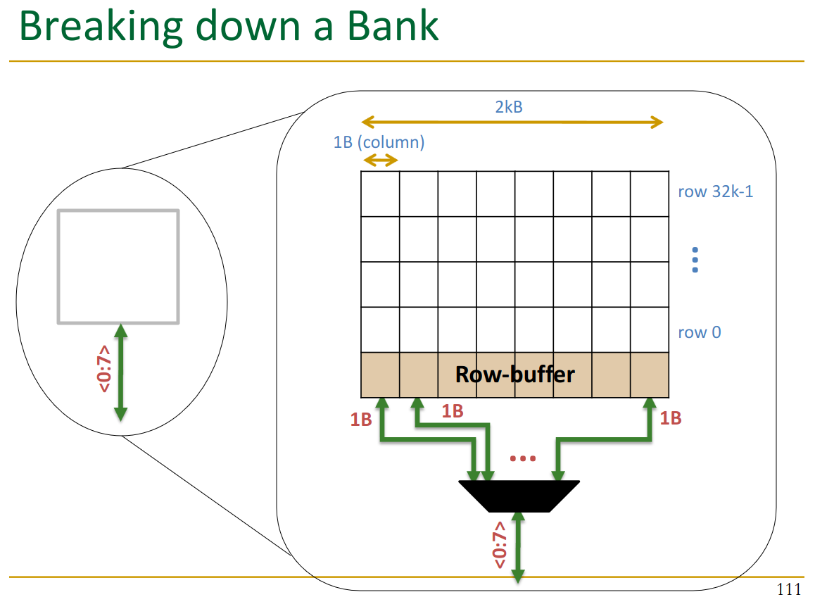
The row-buffer stores an entire row between accesses.
If we detect that we want a column in an already loaded row → 2-3x faster.
- called a row-buffer hit → very important!
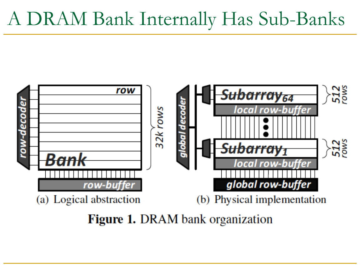
22.5.2 Physical Layout
The view above is only an abstraction. In the real world, such a large array would be too big to be efficient.
Sub-banks: Thus we separate into sub-banks.
22.6 DRAM
A single DRAM cell is made up of transistor and capacitor. These actually store the data.
- small - cannot drive circuits
- reading destroys the state
→ we also need the sense-amplifier. It can be shared accross a bitline though.
Capacitor + Amplifier:
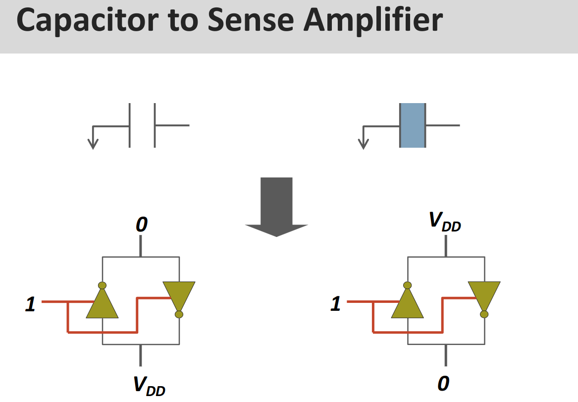
We keep the amplifier in the meta-stable state at . Then the tiny of charge from the capacitor tips the scales.
→ It amplifies the signal to
This also drains / charges the capacitor up again fully, “refreshing” it.
Due to charge leaks, the controller periodically opens a wordline without reading to refresh the data there.
22.6.2 Layout on the Chip
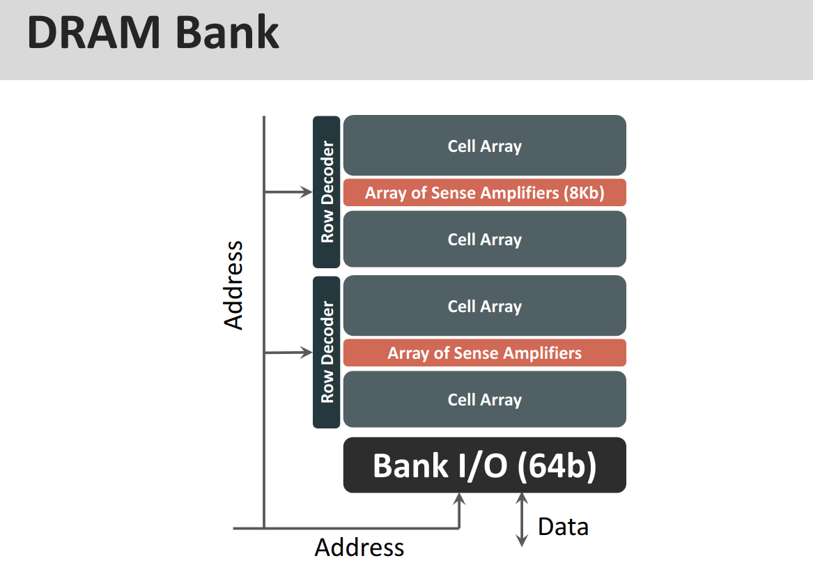
DRAM Bank The entire bank then looks like this:
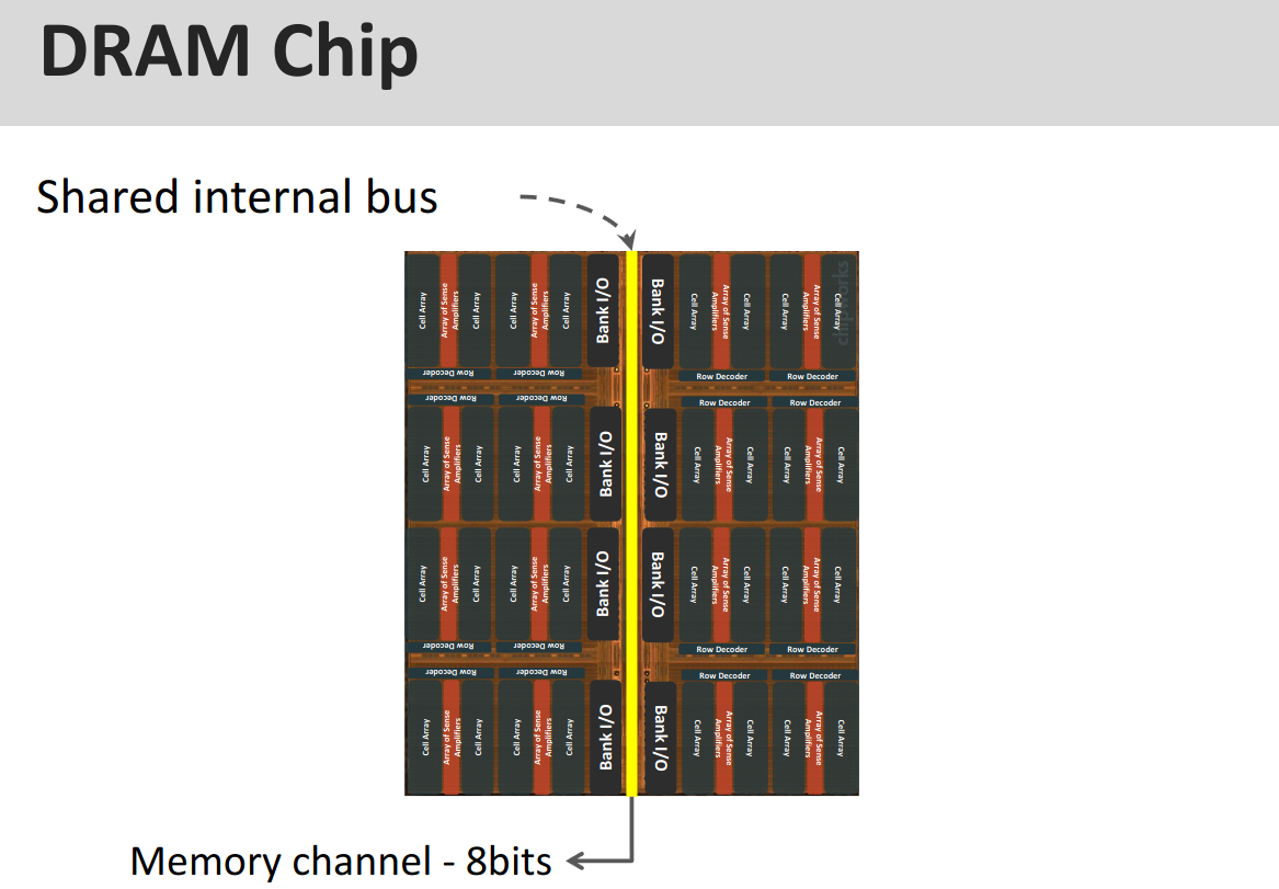
DRAM Chip and the entire chip arranges them
Operation A single operation looks like this (if not row-buffered)
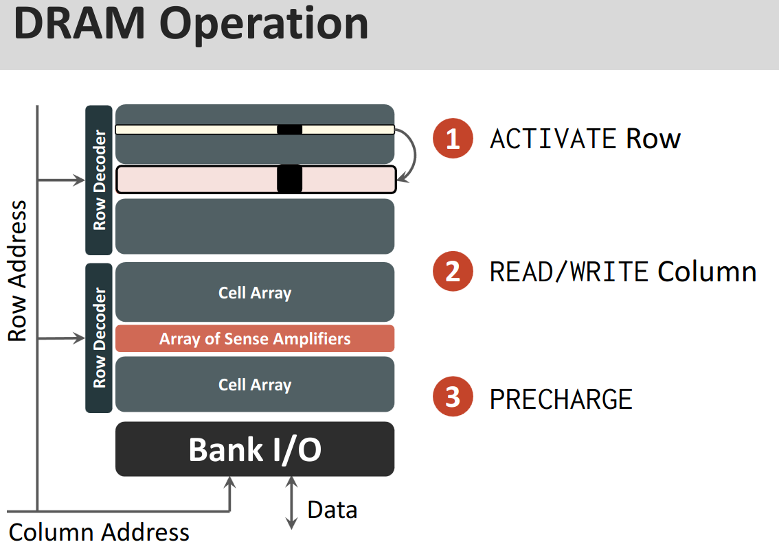
- ACTIVATE
- row decoder
- sense amplifiers
- into the row buffer
- R/W from the column
- Mux selects which column is accessed
- PRECHARGE
- before we can ACTIVATE another row
- write back data into actual array from buffer
- reset all bitlines to
- the row-buffer is empty and idle
22.6.3 Transferring a Cache Block
When we access memory, we don’t actually just read out a 64 bit word into the physical memory.
We always get this entire cache-block, since activating the row takes so much longer than reading from row-buffer, we just store the entire thing in CPU cache.
22.7 SRAM
The longer the bitline, the higher the latency. Thus we split into subarrays, etc..
22.8 PCM (Phase Change Memory)
PCM works by using a glass which reacts and changes phase when exposed to heat.
PCM can be used as a main memory.
→ Intel Optane for example.
Optane can also be used instead of DRAM.