Where combinational circuit’s output depends solely on input, we also need storage / memory. This is where sequential logic comes in.
There’s a hierarchy of storage elements, trading off speed, cost, and volatility:
- Latches and Flip-Flops: Very fast, parallel access. Very expensive (one bit costs tens of transistors). Used for registers and small, fast memory within the processor.
- Static RAM (SRAM): Relatively fast. Expensive (one bit costs 6+ transistors). Used for caches (intermediate memory between the processor and main memory).
- uses 6 transistors in a bistable latch configuration.
- Dynamic RAM (DRAM): Slower; reading destroys the stored content, requiring periodic “refresh.” Cheap (one bit costs one transistor + one capacitor). Used for main memory (RAM). Requires specialized manufacturing processes.
- the capacitor holds the charge, when reading we drain it.
- Other Storage (Flash, Hard Disk, Tape): Much slower, but non-volatile (data persists without power). Very cheap. Used for long-term storage.
Memory Element Types
- Edge-Triggered: A flip-flop is called edge-triggered because it captures data on the clock edge (rising or falling).
- Level-Sensitive: A latch is level-sensitive because its output follows the input whenever the enable signal (WE) is at the active level (high or low, depending on the latch design).
3.1 Keeping State
3.1.1 Basic Element: Cross-Coupled Inverters
By linking up two inverters to themselves in this way, we can persist state - as long as we provide power.
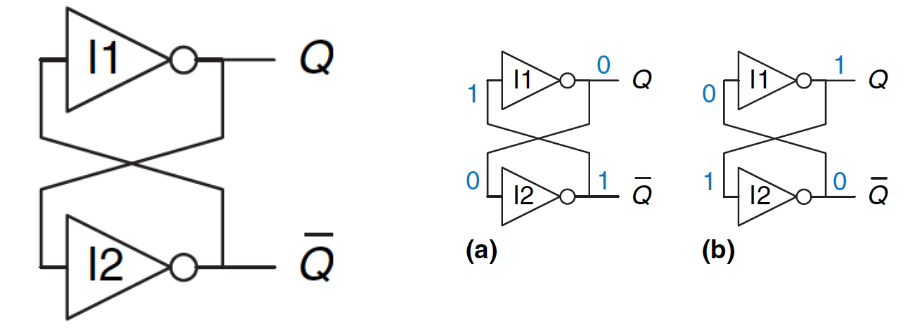
The cross-coupled inverters have two stable states: or . There is also a “metastable” state, in which they oscillate between and .
We need a control mechanism for setting the data though!
3.1.2 R-S Latch
The reset-set latch is built using two cross-coupled NAND gates.
- data is stored at
- and are control inputs
- in idle, both and held at 1 (constant power)
- (set): drive to (keep at 1) to change to 1
- (reset): drive to (keeping at 1) to change to 0
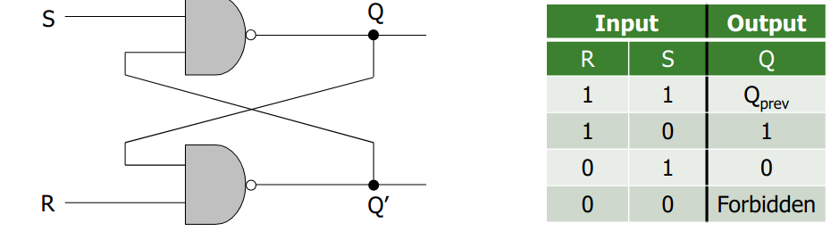
and should not both be at the same time, otherwise we will start to have oscillations (metastable) which will settle into an unpredictable state (depending on timing).
3.1.3 Gated D-Latch
How do we guarantee that and are never at the same time? To solve this, we use a Gated D-Latch which uses some more transistors in exchange for correctness.
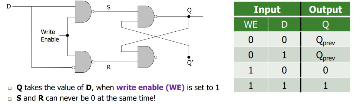
We now have a write-enable input which specifies when to write and a data input.
- WE = 0: The latch holds its current state (Q remains unchanged).
- WE = 1: The latch becomes transparent; Q takes on the value of D (Q = D).
3.1.4 The D Flip-Flop
Why do we need Flip-Flops for FSM? Directly connecting the clock signal to the WE (Write Enable) input of a D latch is problematic for implementing state registers. A D latch is transparent when WE is high: the output Q continuously follows the input D.
This violates the requirement to hold the state constant throughout the clock cycle.
![]()
The challenge is to design a storage element that:
- Samples the input (D) only at the beginning of the clock cycle (e.g., on the rising edge).
- Holds the output (Q) constant for the entire clock cycle, regardless of changes in D.
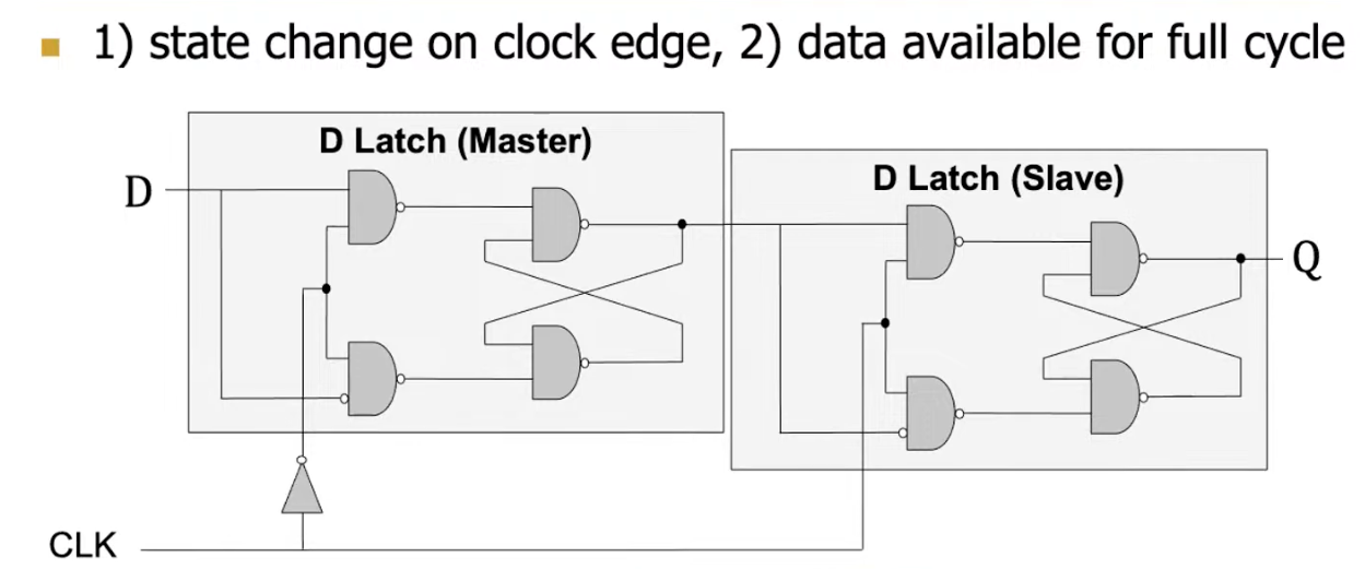
We connect two latches in series, one “master” and one “slave”. By inverting the clock for the first latch, we ensure that it has to have an edge before letting the D propagate to the final Q.
- Clock Low (CLK = 0): The master latch is transparent (its Q follows its D), while the slave latch is holding its previous value. The input D propagates through the master latch to the input of the slave latch.
- Clock High (CLK = 1): The master latch becomes opaque (holds its value), while the slave latch becomes transparent. The value that was present at the input of the slave latch (which was captured by the master latch before the clock went high) is now passed to the output Q.
- Clock Transitions to Low (CLK = 0): The master latch once again becomes transparent allowing the new D input to proagate to the input of the slave. The slave continues to hold and display the previous D input.
3.2 Memory
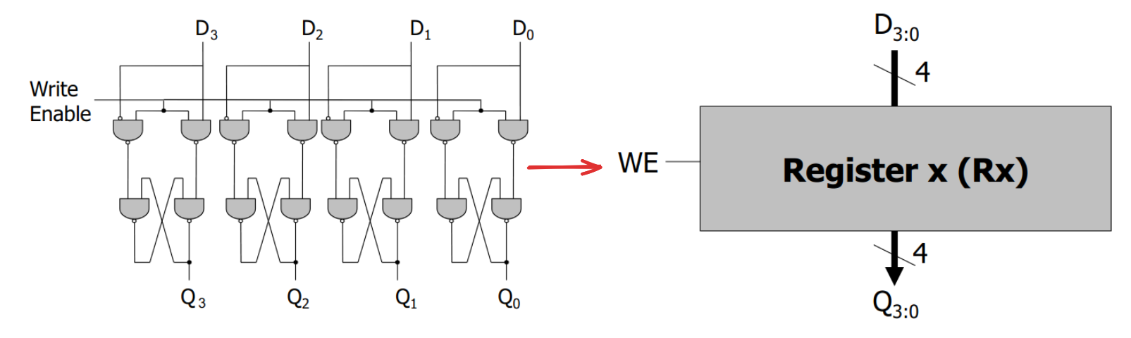
3.2.1 Register
By chaining together D-Latches into a register, we can store multiple bits. We connect all the write-enable signals together.
3.2.2 Memory
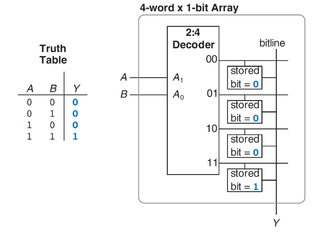
Memory is comprised of locations that can be written to or read from. Each location is indexed with a unique address (4 locations require address bits, use ).
Addressability
Addressability is the number of bits of information stored in each location.
Could be bits, or bits, etc…
The entire space of unique locations is called address space.
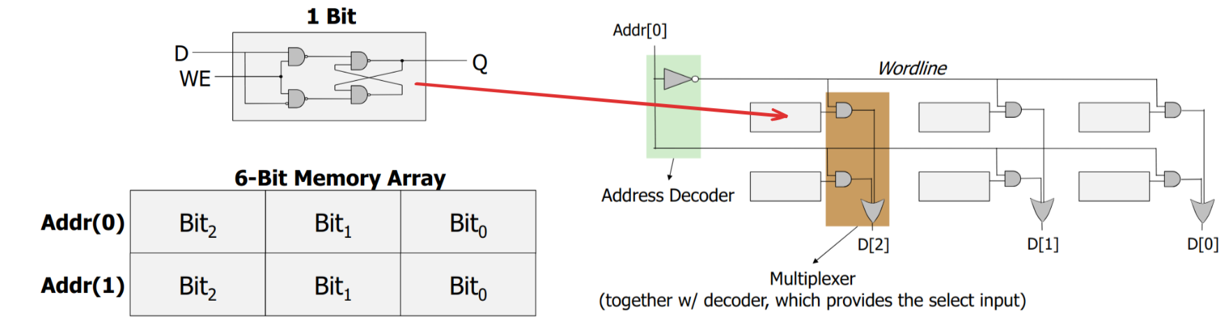
We can arbitrarily expand this, to support more address space. We just have to expand the decoder and multiplexer and add more bit cells.
Reading and writing at bit-level:
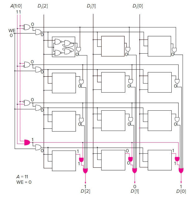
3.2.3 Functions in Memory
By using a LUT (Lookup table), an FPGA can implement any logic function it wishes to.
Each address then corresponds to the function inputs, and in each -bit cell, the output of the function table is stored.